Errata (clarifications and corrections)
2.4 Capacitors (DC)
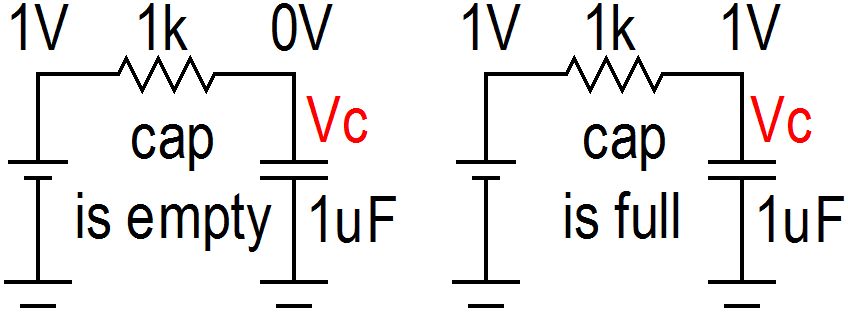
Figure 2.4-1
Another useful equation is rise time. Rise time is defined as the time it takes to change from 10% of the final voltage to 90% of the final voltage. Rise time is approximately 2.2 times the time constant.
2.7 Capacitors (AC) / RC Filter
Plot equation: y=20*log(x) ? x=10(y/20)
when y= -3dB ? x=10(-3/20)
x=0.707 (70.7% of the input voltage)
when y= -20dB ? x=10(-20/20)
x=0.1 (10% of the input voltage)
2.13 Fuses
A fuse disrupts current flow when a maximum current is reached. When the maximum current is exceeded, the exceeded. The fuse breaks an internal connection, usually by melting a conductor.
Low current fuses, in the low mA range, may require special treatment handling when soldered.
2.14 Transformers
A transformer is a combination of two closely coupled inductors. AC current flowing through one inductor (primary) creates a magnetic field. A second inductor (secondary) converts the magnetic field back into AC current. Both inductors are usually wrapped around the same magnetic core (Figure 2.14-1).

Figure 2.14-1
2.15 Common Mode Chokes
Common mode chokes are two inductors combined into one component. Two wires are wound in parallel on a single magnetic core forming a highly coupled 1:1 transformer.
This common mode choke restricts AC current (undesired noise) and allows DC current.
Common mode chokes, on power and ground connections, reduce external electronic noise from entering the electronic assembly.
They also reduce electronic assembly noise from exiting the assembly which could affect other electronic equipment.
This can be crucial for meeting EMC requirements.
3.1 Diodes
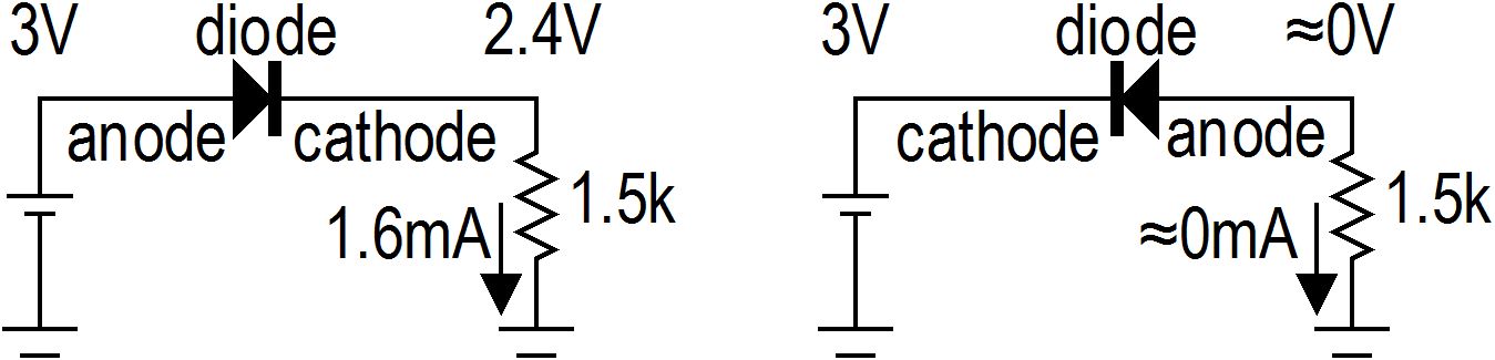
Figure 3.1-1
3.4 Zener Diodes
Zener diodes are designed to provide an accurate reverse voltage drop. In the forward direction, they behave like diodes. In the reverse direction, they limit the current until the Zener knee voltage is reached (Figure 3.4-1).
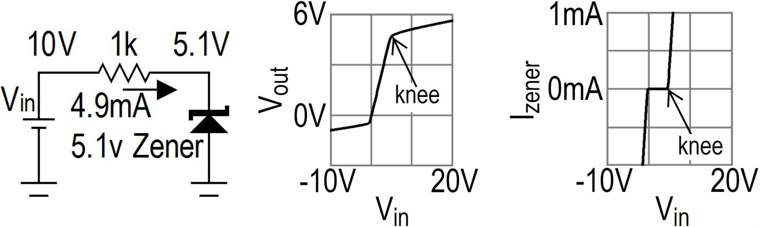
Figure 3.4-1
A 5.1V BZT52C5V1 Zener diode that has a knee voltage at 5.1V. This Zener diode limits the voltage to approximately 5.1V. As the current through the Zener diode increases, the knee voltage increases a small amount (Figure 3.4-2).
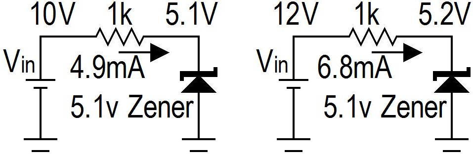
Figure 3.4-2
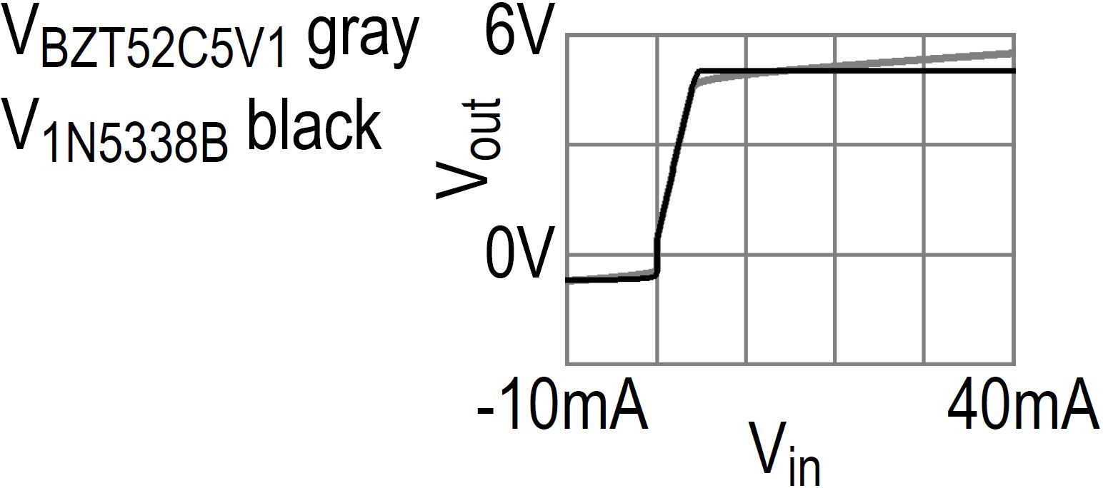
Figure 3.4-3
3.5 FETs (Field Effect Transistors)
Drain voltages are rarely higher than source voltages. When the drain voltage exceeds the source voltage by approximately 0.6V (a diode forward voltage drop), the current flows backwards through the FET. Inserting a diode in series with the FET drain eliminates this problem (Figure 3.5 5).
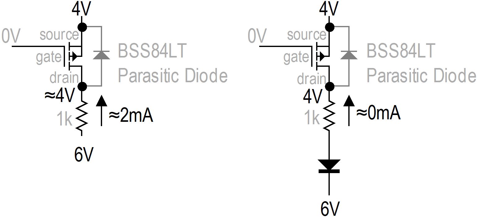
Figure 3.5-5
3.9 Digital Potentiometer
A digital potentiometer provides the ability to electronically change a resistor value (Figure 3.9-1). The resistor value is changed by a micro using SPI communication (see SPI Serial Communication section).
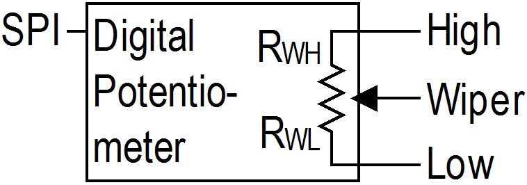
Figure 3.9-1
The Maxim MAX5401 provides a maximum of 100k (resistances ranging from 0 and 100k). It divides this resistance into 256 values.
RWH (Resistance between Wiper and High)
RWL (Resistance between Wiper and Low)
RWH+RWL=100k ohms
SPI sets to 0 -> RWL = 0/255*100k -> RWL = 0 ohms
SPI sets to 1 -> RWL = 1/255*100k -> RWL = ~392.2 ohms
SPI sets to 2 -> RWL = 2/255*100k -> RWL = ~784.3 ohms
SPI sets to 3 -> RWL = 3/255*100k -> RWL = ~1176.5 ohms
...
SPI sets to 255 -> RWL = 255/255*100k -> RWL = 100k ohms
3.10 Optoisolators
The input current does not begin to flow until the input voltage exceeds 1.6V. As the input voltage increases, the input current increases. As the input current increases, the output current increases.
While the output current follows the input current, it is non-linear. The Figure 3.10-1 input current is a straight line. The output current is not straight line.
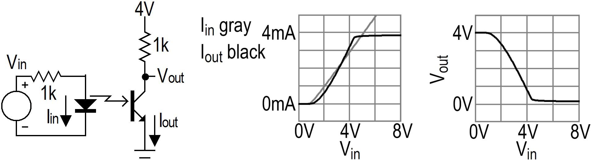
Figure 3.10-1>
4.1 Comparators
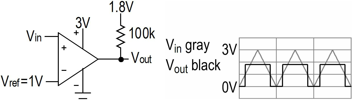
Figure 4.1-5
4.2 Op Amps
When power is initially applied to an op amp, the output is 0V. When the "+" input voltage is larger than the "-" input voltage, the output voltage starts to increase.
4.3 Op Amp Offset
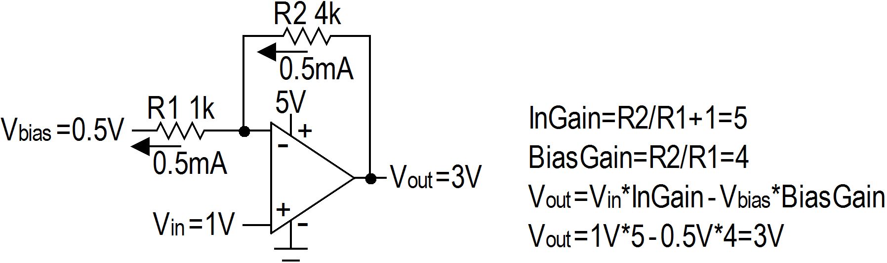
Figure 4.3-1
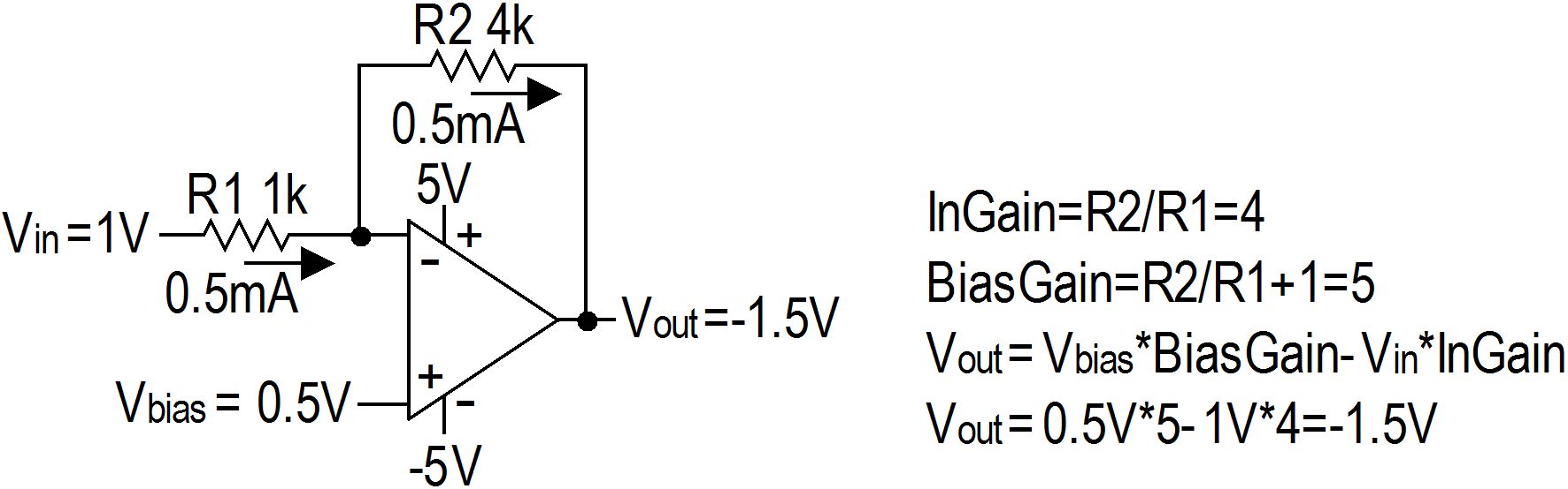
Figure 4.3-2
4.4 Variable Gain / Variable Offset Op Amp
A variable gain op amp (Figure 4.4-1) and variable offset op amp (Figure 4.4-2) are achievable with a digital potentiometer (digital pot). A digital potentiometer resistor value is commonly changed by a micro (see Digital Potentiometer section).
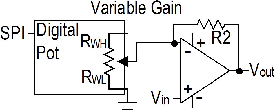
Figure 4.4-1
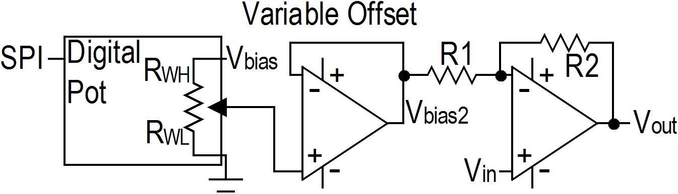
Figure 4.4-2
The variable gain is determined by R2 divided by RWL. The variable offset is determined by Vbias times RWL divided by (RWH+RWL).
The variable gain and variable offset can be combined (Figure 4.4-3). Digital Pot1 is the variable gain and Digital Pot2 is the variable offset.
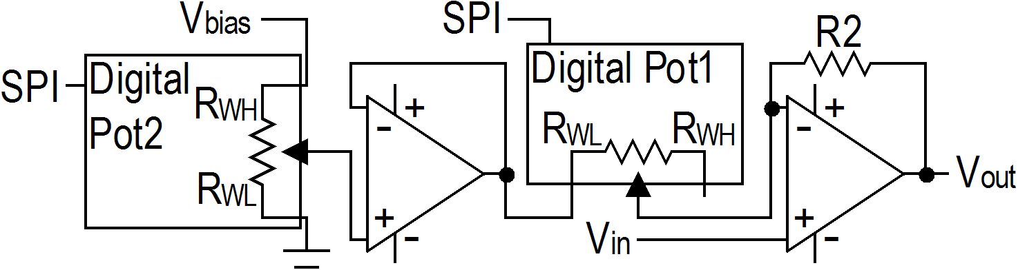
Figure 4.4-3
Without the unity gain op amp between Digital Pot1 and Digital Pot2, Digital Pot2 would affect the gain.
4.7 Differential Input / Output Op Amp Filtering
Sometimes a sensor detects electronic noise. Filtering a differential input / output signal can help.
A 200k resistor with a 0.1uF capacitor has a 7.96Hz cutoff frequency.
Cutoff frequency=1/(2*pi*R*C)
Cutoff frequency=1/(2*pi*200k*0.1�f)=7.96Hz
For this differential input / output op amp configuration, splitting the 200k resistor into two 100k resistors (R4 and R5) is necessary for a differential configuration (Figure 4.7 1).
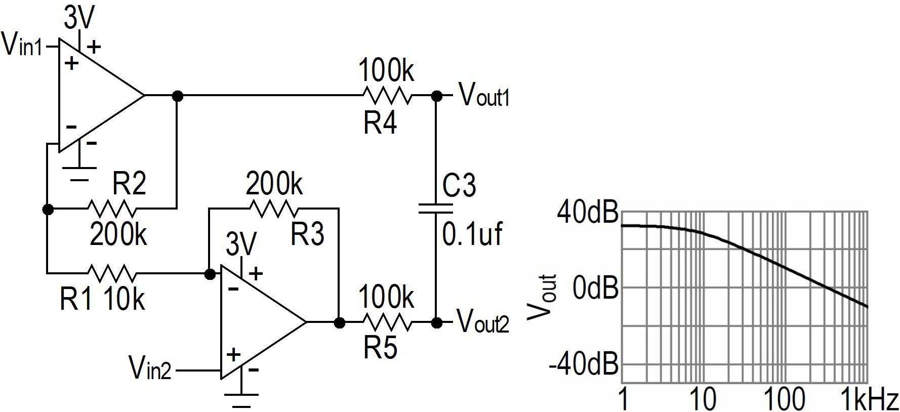
Figure 4.7-1
4.8 Rail to Rail Op Amp
Op amp output voltages can become non-linear as the outputs approach the power rail. In Figure 4.8-1, as Vin approaches 3V (the power rail is 3V) Vout stops following Vin.
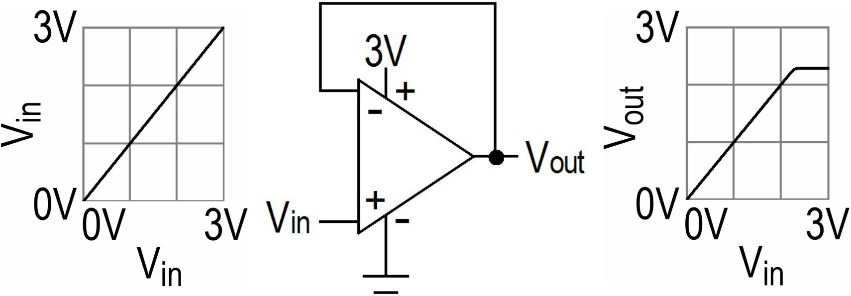
Figure 4.8-1
Rail-to-rail op amps allow output voltages to approach the voltage rails with minimal effect (Figure 4.8-2).
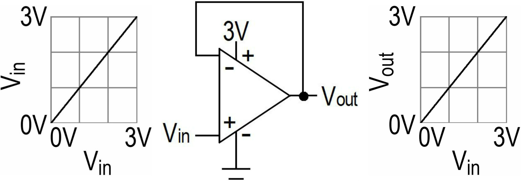
Figure 4.8-2
4.9 Sensors / Constant Current / Voltage
Some sensors are a resistor bridge. Pressure sensors are one example. As the pressure changes, the resistance changes.
In Figure 4.9-1, the output is a differential output. Two different pressures result in two different differential voltage outputs.
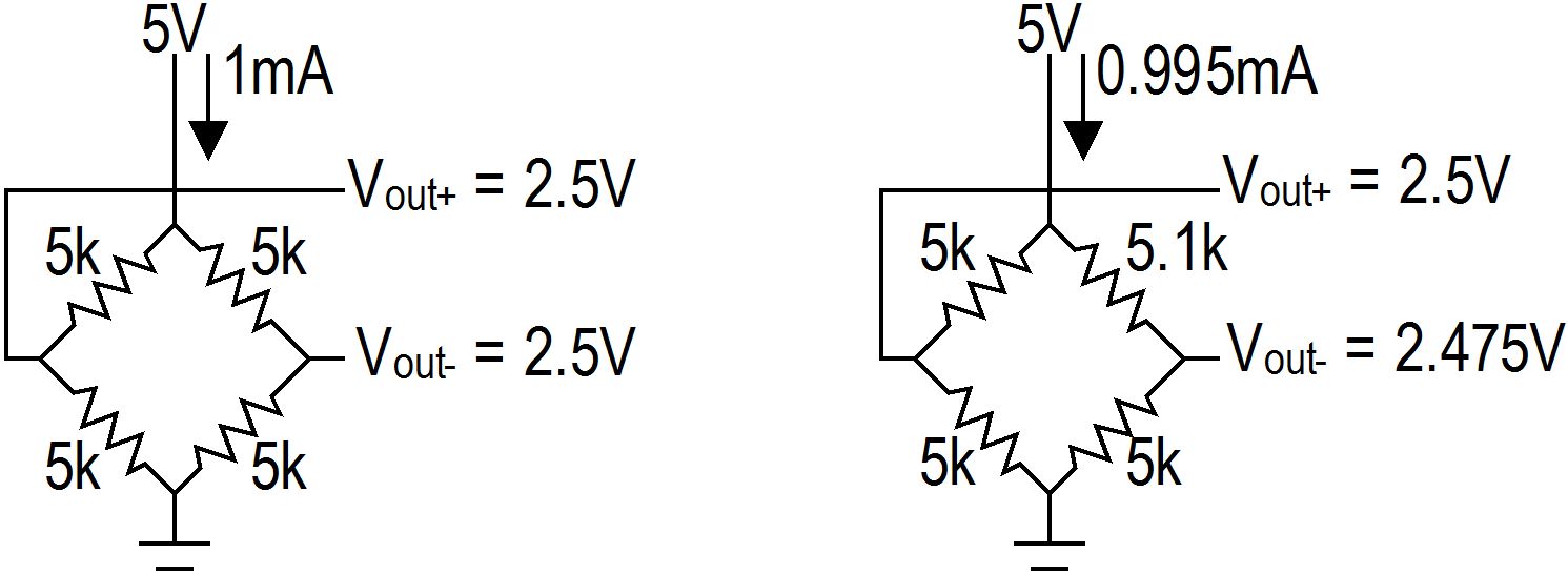
Figure 4.9-1
When two pressure sensors are connected in series, a pressure change in one sensor affects the voltage output from the second pressure sensor. In Figure 4.9-2, when R1 is changed from 4.8k to 4.9k, Vout2+ - Vout2- changes from 125.7mV to 125.4mV. This results in an error as there was no pressure change to the second sensor.
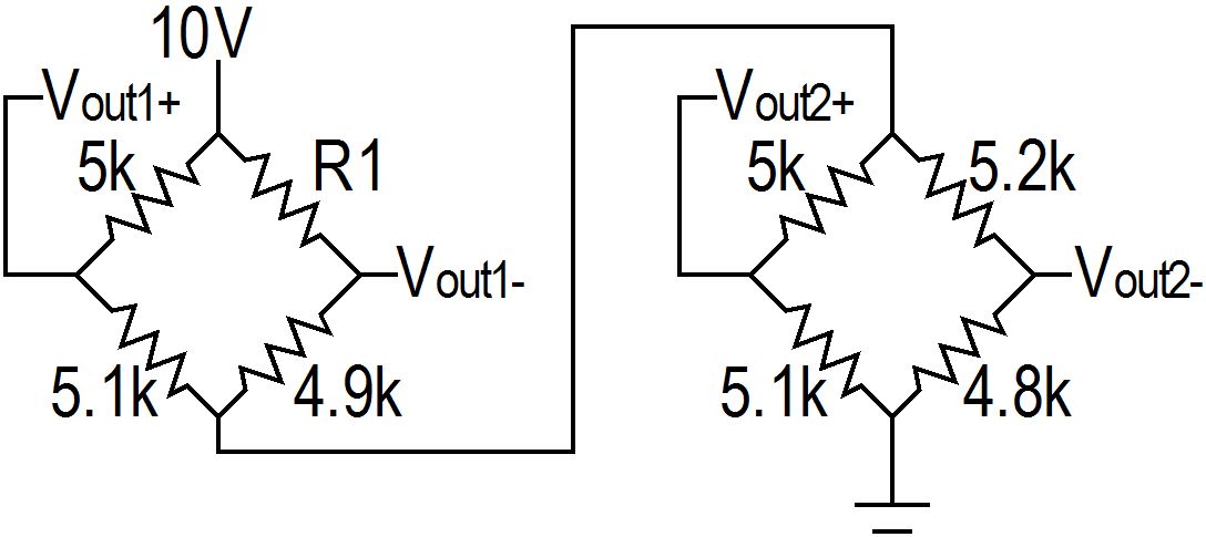
Figure 4.9-2
Using a constant current source for sensors in series eliminates this problem (Figure 4.9 3). When R1 is changed from 4.8k to 4.9k, Vout2+ - Vout2- does not change. It stays at 123.1mA.
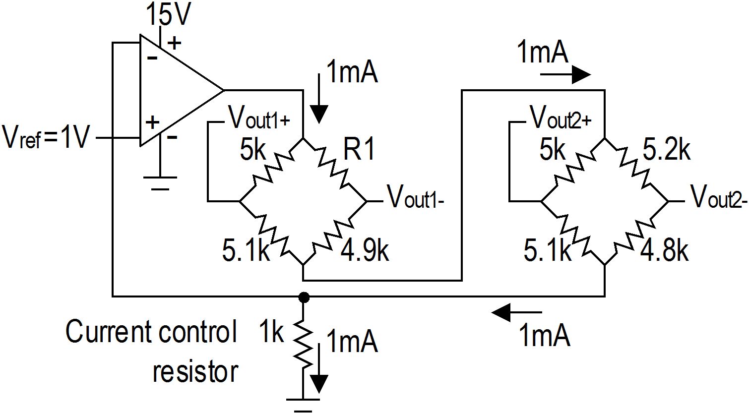
Figure 4.9-3
Low power op amps may have limited output current. A FET could provide the extra current (Figure 4.9 4).
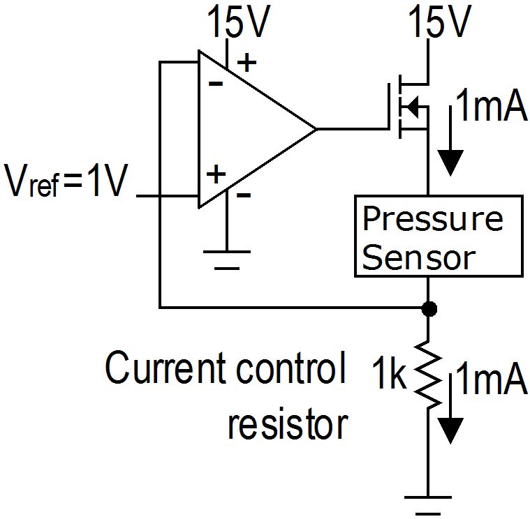
Figure 4.9-4
When the sensors are placed in parallel, there is no need for constant current. Pressure changes to one sensor will not affect the other sensor output.
The decision to use, or not use, a constant current source is dependent on the requirements. Sensors in series with a constant current source will consume the least amount of current.
4.13 Voltage Supervisors
The Intersil ISL88002IE29Z-T and the Analog Devices ADM803SAKS detect when the voltage is below 2.92V. When this occurs, their output is 0V. This output is connected to a micro reset input. The 0V resets the micro.
4.10 Instrumentations Amps
An instrumentation amp has close to zero current into the inputs. This eliminates the constraints of source impedance as described in the Differential Op Amp section.
The instrumentation amp outputs may not be linear when the inputs approach either power rail. Ensuring the inputs do not approach the power rails ensure a valid output.
One common constraint for most ICs is the "+" and "-" inputs cannot exceed the power rails by more than 0.5V. If the IC is powered by 3V the "+" and "-" inputs must be greater than -0.5V and less than 3.5V.
Exceeding this limit can result in damage to the IC.
The INA826 does not have this restriction. It can handle up to a 40V input beyond the power rails without any damage. The INA826 may not operate properly in this state, but it will not be damaged.
5.1 Digital Component Basics
Digital component I/O (inputs / outputs) is either a "1" or "0". Electronic noise has close to zero effect on the results.
When an IC (integrated circuit) is powered by 3.3V a "1" equals 3.3V and a "0" equals 0V. When powered by 5V, a "1" equals 5V and a "0" equals 0V.
...
When a mechanical switch changes position (for example on / off), the inputs are momentarily floating. After the switch makes contact, the switch output bounces. Digital logic gates eliminate this problem (Figure 5.1 4).
5.3 Bytes, Integers, Long, Unsigned
Bits are often in groups of 8, 16, or 32. The MSB (most significant bit) is on the left. The LSB (least significant bit) is on the right.
unsigned: all bits are a positive number
signed: the MSB is a sign bit, the remainder are a number
unsigned byte (also known as a char) 8 bits
01111111b=0x7F=127
10000000b=0x80=128
11111111b=0xFF=255
signed byte 8 bits, 1 sign bit and 7 data bits
01111111b=0x7F=127
10000000b=0x80= -128
11111111b=0xFF= -1
unsigned integer 16 bits
0000000000000001b=0x0001=1
0111111111111111b=0x7FFF=32767
1000000000000000b=0x8000=32768
1111111111111110b=0xFFFE=65534
1111111111111111b=0xFFFF=65535
signed integer (int) 1 sign bit and 15 data bits
0000000000000001b=0x0001=1
0111111111111111b=0x7FFF=32767
1000000000000000b=0x8000= -32768
1111111111111110b=0xFFFE= -2
1111111111111111b=0xFFFF= -1
unsigned long 32 bits
00000000000000000000000000000001b=0x00000001=1
01111111111111111111111111111111b=0x7FFFFFFF=2147483647
10000000000000000000000000000000b=0x80000000=2147483648
11111111111111111111111111111111b=0xFFFFFFFF=4294967295
signed long (long) 1 sign bit and 31 data bits
00000000000000000000000000000001b=0x00000001=1
01111111111111111111111111111111b=0x7FFFFFFF=2147483647
10000000000000000000000000000000b=0x80000000= -2147483648
11111111111111111111111111111111b=0xFFFFFFFF= -1
5.5 ADCs (Analog to Digital Converters)
ADCs convert a voltage (Vin) into a binary number. The ADC requires an input reference voltage (Vref). Vin compared to Vref results in a binary number that is readable by micro.
A two bit ADC converts Vin into a two bit binary number (Figure 5.5-1).
Vref=9V
Vin=0V -> 0V/9V*3 = 0 = 00b
Vin=3V -> 3V/9V*3 = 1 = 01b
Vin=6V -> 6V/9V*3 = 2 = 10b
Vin=9V -> 9V/9V*3 = 3 = 11b
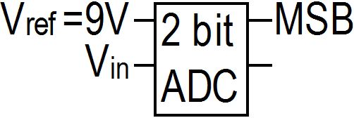
Figure 5.5-1
A four bit ADC converts Vin into a four bit binary number (Figure 5.5-2).
Vref=3V
Vin=0.0 -> 0.0V/3V*15 = 0 = 0000b
Vin=0.2 -> 0.2V/3V*15 = 1 = 0001b
Vin=0.4 -> 0.4V/3V*15 = 2 = 0010b
Vin=0.6 -> 0.6V/3V*15 = 3 = 0011b
Vin=0.8 -> 0.8V/3V*15 = 4 = 0100b
Vin=1.0 -> 1.0V/3V*15 = 5 = 0101b
Vin=1.2 -> 1.2V/3V*15 = 6 = 0110b
Vin=1.4 -> 1.4V/3V*15 = 7 = 0111b
Vin=1.6 -> 1.6V/3V*15 = 8 = 1000b
Vin=1.8 -> 1.8V/3V*15 = 9 = 1001b
Vin=2.0 -> 2.0V/3V*15 = 10 = 1010b
Vin=2.2 -> 2.2V/3V*15 = 11 = 1011b
Vin=2.4 -> 2.4V/3V*15 = 12 = 1100b
Vin=2.6 -> 2.6V/3V*15 = 13 = 1101b
Vin=2.8 -> 2.8V/3V*15 = 14 = 1110b
Vin=3.0 -> 3.0V/3V*15 = 15 = 1111b
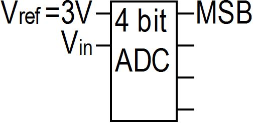
Figure 5.5-2
5.6 DACs (Digital to Analog Converters)
DACs convert a binary number into a voltage (Vout). The DAC requires an input reference voltage (Vref). The binary number produces a Vout that is compared to Vref. The binary number can be generated by a micro.
A four bit DAC converts a four bit binary number into Vout (Figure 5.6-1).
Vref=3V
0000b -> Vout=3V/15*0 = 0.0V
0001b -> Vout=3V/15*1 = 0.2V
0010b -> Vout=3V/15*2 = 0.4V
0011b -> Vout=3V/15*3 = 0.6V
0100b -> Vout=3V/15*4 = 0.8V
0101b -> Vout=3V/15*5 = 1.0V
0110b -> Vout=3V/15*6 = 1.2V
0111b -> Vout=3V/15*7 = 1.4V
1000b -> Vout=3V/15*8 = 1.6V
1001b -> Vout=3V/15*9 = 1.8V
1010b -> Vout=3V/15*10 = 2.0V
1011b -> Vout=3V/15*11 = 2.2V
1100b -> Vout=3V/15*12 = 2.4V
1101b -> Vout=3V/15*13 = 2.6V
1110b -> Vout=3V/15*14 = 2.8V
1111b -> Vout=3V/15*15 = 3.0V
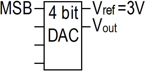
Figure 5.6-1
5.10 Firmware / Software Code
Texas Instruments MSP430 code
C code (readable):
uint8_t ucValue=1;
uint16_t uiValue=2;
uint16_t uiSum=ucValue+uiValue;
End result: uiSum = 3
Assembler code (somewhat readable):
mov.b #0x1, R10
mov.w #0x2, R11
mov.b #R10, R8
add.w #R11, R8
End result: R8 = 3
Binary number code (challenging to read) stored in FLASH:
0x6DC2: 0x435A
0x6DC4: 0x432B
0x6DC6: 0x4A48
0x6DC8: 0x5B08
End result: R8 = 3
Texas Instruments MSP430 code with comments
C code: uint8_t ucValue=1;
//Assigns the number 1 to ucValue.
Assembler code: mov.b #0x1, R10
//Places the number 1 into register R10.
Binary number: 0x6DC2: 0x435A
//Number 0x435A (instruction) is at FLASH address 0x6DC2. Instruction places number 1 into R10.
C code: uint16_t uiValue=2;
//Assigns the number 2 to uiValue.
Assembler code: mov.w #0x2, R11
//Places the number 2 into register R11.
Binary number: 0x6DC4: 0x432B
//Number 0x432B (instruction) is at FLASH address 0x6DC4. Instruction places number 2 into R11.
C code: uint16_t uiSum=ucValue+uiValue;
//Assigns uiSum to be sum of ucValue and uiValue.
Assembler code: mov.b #R10, R8
//Moves a copy of register R10 into register R8.
Binary number: 0x6DC6: 0x4A48
//Number 0x4A48 (instruction) is at FLASH address 0x6DC6. Instruction moves a copy of R10 into R8.
Assembler code: add.w #R11, R8
//Add register R11 to register R8.
Binary number: 0x6DC8: 0x5B08
//Number 0x5B08 (instruction) is at FLASH address 0x6DC8. Instruction adds R11 to R8.
5.12 SPI Serial Communication
Serial communication is access to one bit at a time.
SPI (Serial Peripheral Interface) is a standard serial communication protocol. It is comprised of one master and one, or more, slaves. The data is an MSB format.
A master outputs SpiClk (clock), SpiMoSi (master out slave in), and CS (chip select). A slave outputs SpiMiSo (master in slave out).
The first byte on SpiMoSi is an op code (00000011b) of 0x03 (indicates to the slave this is a write command). The second byte is an address of 0x16 (indicates to the slave the location to place the first data byte). The third and fourth byes are data bytes 0x4A and 0x66 placed in the slave device.
In Figure 5.12-2, the first SpiMoSi byte is an op code of 0x05 (indicates to the slave this is a read command). The second SpiMoSi byte is an address of 0x31. The third and fourth byes are data bytes 0x8E and 0x47 from the slave on SpiMiSo (from slave addresses 0x31 and 0x32).
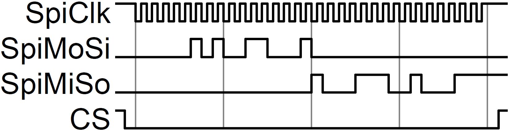
Figure 5.12-2
When additional SpiClks are sent, the slave continues to place bytes on SpiMiSo. A third data byte would be from slave address 0x33.
5.13 I2C Serial Communication
The Start occurs with the master changing SDA from "1" to "0" while SCL is "1". The Stop occurs with the master changing SDA from "0" to "1" while SCL is "1". All other SDA changes occur while SCL is "0" (Figure 5.13-1).
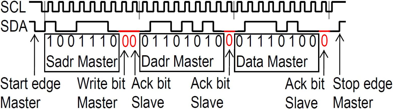
Figure 5.13-1
In Figure 5.13-2, the slave address is 0x2D, the data address is 0x4B, and the data is 0x1C. There could be additional bytes sent after the 0x1C.
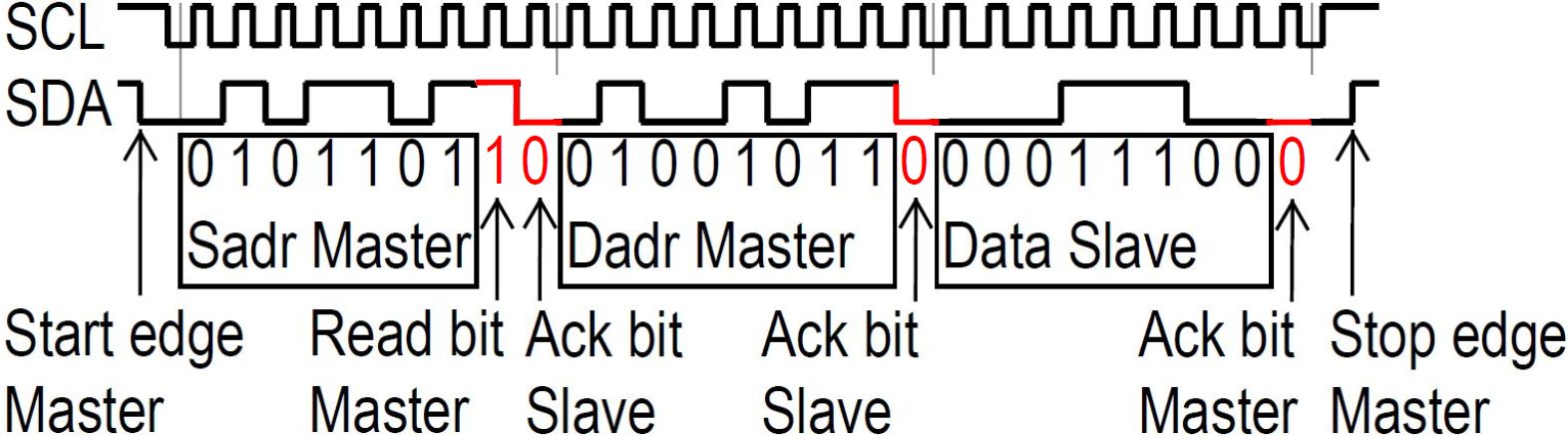
Figure 5.13-2
5.14 RS-232 / RS-485 Serial Communication
For odd parity, the number of "1" bits, including the parity bit must be an odd number. In Figure 5.14-3 the parity bit is "1" for 0x03 (00000011b), and the parity bit is "0" for 0x64 (01100100b).
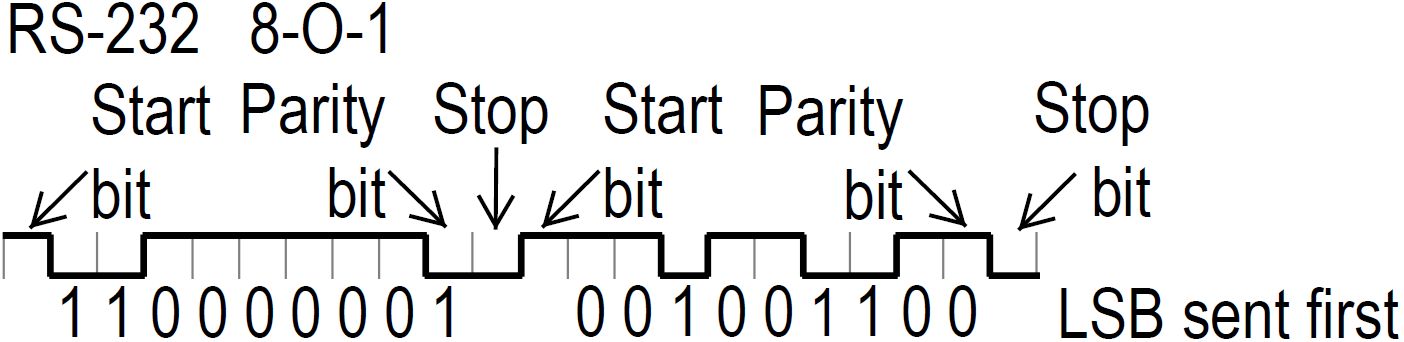
Figure 5.14-3
A variation of RS-232 is to use full-duplex or half-duplex. Full-duplex uses one wire for transmit and another wire for receive. Half-duplex uses the same wire for transmit and receive (Figure 5.14-4).
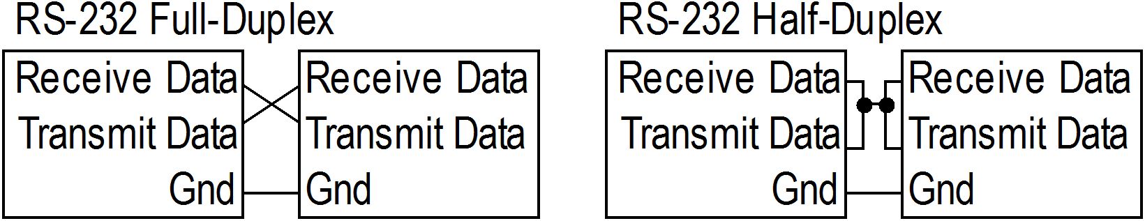
Figure 5.14-4
Over long distances, noise can affect the performance. To help reduce this problem, the RS-422 (two wire, differential communication) became a standard. RS-422 is the same as RS-232 except for the two wire connection.
RS-485 is an extension of RS-422 (Figure 5.14-5). An RS-485 allows connecting multiple devices to the same pair of wires by including a device address with the communication.
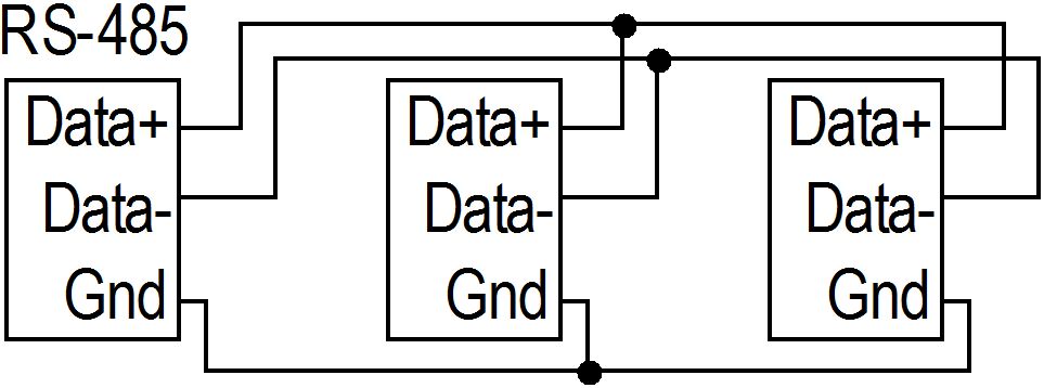
Figure 5.14-5
For a "1", the Data+ wire is a higher voltage than the Data- wire. For a "0" the Data+ wire is a lower voltage than the Data- wire.
Communicating over a long length of wire with RS 232 and RS-485 can cause voltage reflections. The reflection amplitude can be reduced by placing a terminating resistor across the two wires.